RC4 Decryption Hardware Written in Verilog for an FPGA
FPGA Verilog Decryption Parallel Processing Quartus ModelSim
Hardware Design
Summary
This project involved developing a digital circuit that integrated multiple on-chip memories, focusing on creating an RC4 Decryption circuit. It included designing a decryption circuit, constructing foundational components, and an ambitious extension to create an RC4 cracking circuit using a ‘brute-force’ strategy. The project provided hands-on experience in digital circuit design and deepened understanding of cryptographic algorithms. It marked a significant milestone, showcasing proficiency in complex digital circuit and cryptographic algorithm design and implementation.
Description
In this project, I gained practical experience in developing a digital circuit that integrated multiple on-chip memories. The primary goal was to create an RC4 Decryption circuit, a cryptographic algorithm used for stream ciphers. Although RC4 was previously widely used for encrypting web traffic and other applications, security concerns have led to its replacement by more secure variants for reasons that become apparent within this project. This project provided a valuable opportunity to explore the design of digital circuits that heavily rely on on-chip memory and laid the foundation for potential implementations of more secure RC4 variants.

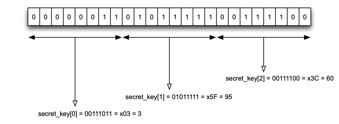
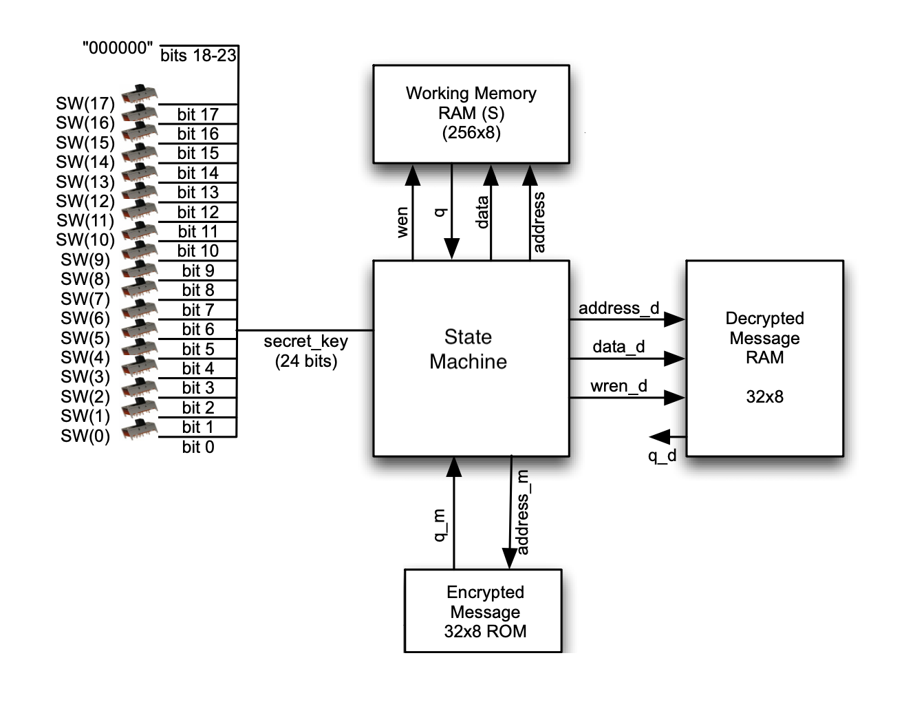
The initial task involved designing an RC4 decryption circuit capable of decrypting messages using a secret key. This secret key was obtained from a bank of switches on the hardware board, while the encrypted message was provided through a ROM initialization file.

This task involved designing hardware capable of executing the RC4 encryption algorithm.
for i = 0 to 255 {
  s[i] = i;
}
j = 0;
for i = 0 to 255 {
  j = (j + s[i] + secret_key[i mod keylength] ) mod 256
  swap values of s[i] and s[j]
}
i = 0, j=0
for k = 0 to message_length-1 {
  i = (i+1) mod 256
  j = (j+s[i]) mod 256
  swap values of s[i] and s[j]
  f = s[ (s[i]+s[j]) mod 256 ]
  decrypted_output[k] = f xor encrypted_input[k]
}
Subsequently, the focus shifted to building the basic components necessary for the decryption circuit’s operation. This phase aimed to create a functional foundation for the subsequent stages of the project.

In an ambitious extension of the project’s scope, we embarked on developing an RC4 cracking circuit. This circuit employed a ‘brute-force’ attack strategy, systematically cycling through the entire keyspace until a successful decryption occurred, thereby achieving the project’s primary objective.
The opportunity was taken to explore the creation of multiple functional units capable of parallel processing. This innovative approach aimed to enhance the project’s capabilities by concurrently cycling through separate portions of the keyspace, significantly accelerating the RC4 cracking process.
This project provided hands-on experience in digital circuit design and the effective utilization of on-chip memory. It also deepened my understanding of cryptographic algorithms and their vulnerabilities. Its successful completion marked a significant milestone in my academic and practical journey, demonstrating proficiency in designing and implementing complex digital circuits and cryptographic algorithms.